
A New record in fabrication of GaN based HEM-Transistor reported by IMEN researcher
06 September 2019 – Taiwan’s National Chiao Tung University and Universiti Kebangsaan Malaysia (UKM) have used ferroelectric materials to create normally-off tri-gate gallium nitride (GaN) metal–insulator–semiconductor high-electron-mobility transistors (MIS-HEMTs) [Chia-Hsun Wu et al, IEEE Transactions on Electron Devices, published online 8 July 2019]. The researchers claim the lowest reported specific on-resistance for normally-off GaN transistors with breakdown voltages greater than 650V.
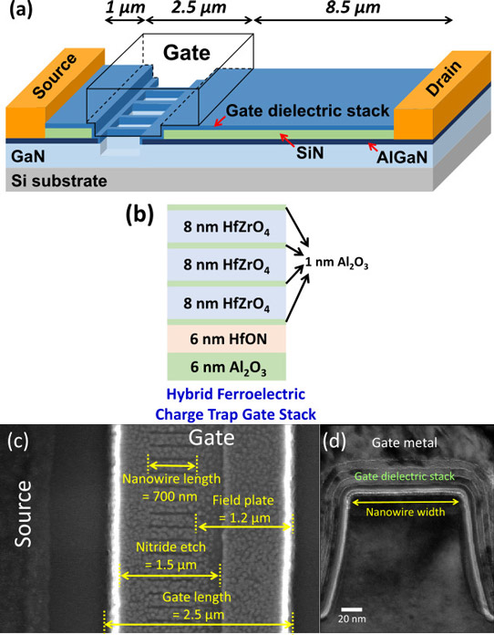
A hafnium oxynitride (HfON) ferroelectric layer in the gate stack was designed to trap charge that shifted the threshold voltage of the transistor to positive values, giving normally-off behavior – i.e. a low current flow at 0V gate potential. Normally-off behavior is desired to reduce power consumption, and in power applications to provide fail-safe operation with simpler circuits. A key trade-off in such devices is between low on-resistance and high breakdown voltage.
The tri-gate structure improved electrostatic control of current flow in the channel by wrapping the gate stack around fins etched out of the channel material.
The III-nitride materials were applied to silicon substrates using metal-organic chemical vapor deposition (MOCVD) to give a 20nm aluminium gallium nitride (Al0.3Ga0.7N) top barrier, 300nm GaN channel and 3μm carbon-doped GaN buffer. Carbon doping of GaN has been found to make it highly resistive.
source : http://www.semiconductor-today.com/news_items/2019/aug/nctu-280819.shtml