MICROELECTRONICS PACKAGING AND MATERIALS (MIPAC) LAB.
A research lab specializing in electronic materials and packaging, with over 20 years of industry collaboration in semiconductors, interconnections, and high-reliability package development.
Head of Laboratory
Prof. Dato'. Dr. Burhanuddin Yeop Majlis
burhan@ukm.edu.my
PIC Laboratory
Anezah Marsan
anezahmarsan@ukm.edu.my
PIC Laboratory
Mohd Faizal Aziz
faizal_imen@ukm.edu.my
EQUIPMENT / FACILITIES
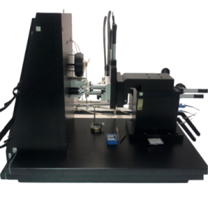
NANOINDENTER
A high-precision instrument used to measure mechanical properties of materials at the micro- and nanoscale, such as hardness, elastic modulus, and creep behavior
How it works Operates by pressing a sharp diamond tip (indenter) into the surface of a sample with a controlled force or displacement. Records the load–displacement curve, which is analyzed to extract mechanical properties based on depth and resistance to indentation.
Key features:
High spatial resolution for localized mechanical measurement.
Automated testing with accurate load and displacement control.
Capable of testing thin films, coatings, and small volumes of material.
Provides quantitative data without the need for extensive sample preparation.
Applications:
Characterization tools of localized micro and nano mechanical properties of solid materials
INFINITEFOCUS MEASUREMENT 3D SURFACE PROFILER
Alicona InfiniteFocus is a high-resolution optical 3D surface profile measurement system.
How it works Based on focus variation technology, the system combines the small depth of focus of an optical system with vertical scanning to generate high-resolution 3D topography and true-color images. Surface height data is obtained by detecting sharpness contrast across different focal planes.
Key features:
Non-contact, high-resolution 3D profile measurement.
Large vertical range with nanometer-level vertical resolution.
Suitable for steep flank and complex geometries.
Applications:
Qualitative, quantitative and stereometry characterization tools for solid surface topography, morphology and texture.
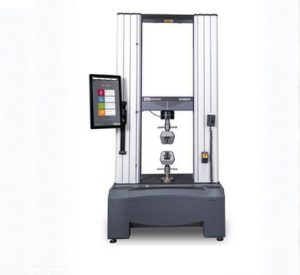
A computer-controlled testing system designed to evaluate the mechanical properties of materials, such as tensile, compression, flexural, and shear strength.
How it works Operates by applying controlled force or displacement to a test specimen while measuring the resulting stress, strain, and deformation. Uses low load cells (2.5N – 2kN) and extensometers to record force and elongation, with results displayed and analyzed through dedicated software.
Key features:
High precision low load cells with wide force capacity range.
Non-destructive and destructive testing capabilities.
Applications:
Characterization tools of mechanical properties of solid materials
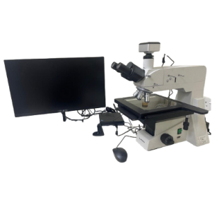
DIGITAL MICROSCOPE
A digital microscope is an optical imaging device that uses a digital camera and display screen to magnify and capture images of small objects with high resolution.
How it works It captures magnified images through optical lenses, then converts them into digital signals via a built-in camera. The images are displayed on a monitor allowing real-time observation and analysis.
Key features:
High-resolution imaging with digital zoom.
Live image/video display and recording capability.
Easy image sharing and documentation.
Applications:
Material science (surface morphology, fracture analysis, coating inspection).
A reflow oven is a thermal processing equipment used to solder surface-mount components onto printed circuit boards (PCBs) by melting solder paste.
How it works The PCB with applied solder paste and components passes through controlled heating zones. The solder paste melts (reflows) and solidifies, creating strong electrical and mechanical connections. Heating follows a specific temperature profile (preheat, soak, reflow, cooling) to ensure reliable solder joints.
Key features:
Multiple heating zones with precise temperature control.
Uniform heat distribution for consistent soldering quality.
Programmable thermal profiles to suit different solder materials and PCB designs.
Applications:
Assembly of electronic circuit boards
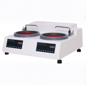
GRINDER / POLISHER
A grinder/polisher is a lab instrument used to prepare metallographic, ceramic, or electronic material samples by grinding and polishing to achieve a smooth, flat surface for analysis.
How it works Uses rotating abrasive surfaces/discs with controlled speed and pressure. Progressive use of finer abrasives removes scratches and achieves mirror-like finishes.
Key features:
Adjustable rotation speed and pressure.
Multiple disc or platen options for different materials.
Water supply system to reduce heat and prevent damage.