Product Details
UKM research instrumentation
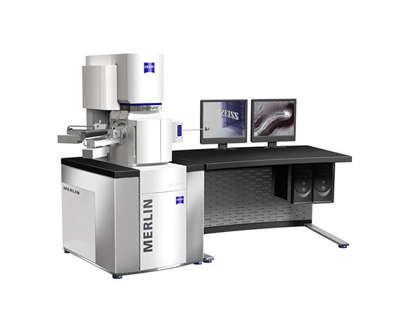
Field Emission Scanning Electron Microscope (FESEM) – MERLIN
Instrument information
Overview
Resolution : 0.8nm @ 15 kV / 1.4nm @ 1 kV / 0.6nm @ 30 kV (STEM mode)
Magnification : 12 – 2,000,000x
Field emission scanning electron microscopy (FESEM) provides topographical and elemental information at magnifications of 10x to 300,000x, with virtually unlimited depth of field. Compared with convention scanning electron microscopy (SEM), field emission SEM (FESEM) produces clearer, less electrostatically distorted images with spatial resolution down to 1 1/2 nanometers which is three to six times better.
Other features of field emission scanning electron microscopy (FESEM) include:
- The ability to examine smaller-area contamination spots at electron accelerating voltages compatible with energy dispersive spectroscopy (EDS).
- Reduced penetration of low-kinetic-energy electrons probes closer to the immediate material surface.
- High-quality, low-voltage images with negligible electrical charging of samples (accelerating voltages ranging from 0.5 to 30 kilovolts).
- Essentially no need for placing conducting coatings on insulating materials.
For ultra-high-magnification imaging, we use in-lens FESEM. In-lens field emission scanning electron microscopy (In-Lens FESEM) provides topographical information at magnifications of 250x to 1,000,000x, with virtually unlimited depth of field. In-lens FESEM produces clearer, less electrostatically distorted images than SEM, with spatial resolution down to 0.6 nanometers – three times better than regular FESEM and 10 times better than conventional SEM.
Instrument information
Applications
Instrument information
Sample Requirements
Instrument information
Typical Results
Instrument information
Price List
| Analysis Code | Type of Analysis | UKM | Non-UKM |
|---|---|---|---|
| SEM 01 | Imaging | RM150/analysis | RM400/analysis |
| SEM 02 | Imaging + EDX | RM200/analysis | RM550/analysis |
| SEM 03 | Imaging + EDX + Mapping | RM250/analysis | RM300/analysis |