Product Details
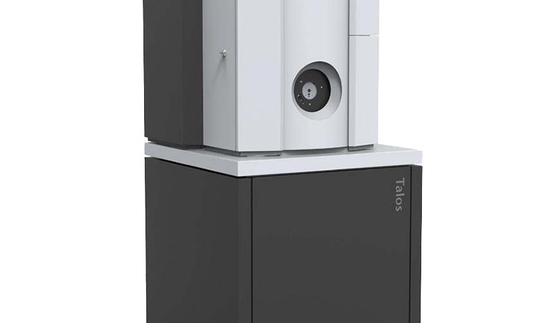
UKM research instrumentation
Transmission Electron Microscope (TEM)
BrandTalos L120C
Model-
LocationLevel 3, i-CRIM Centralised Lab, Centre for Natural and Physical Laboratory Management UKM (ALAF-UKM), Research Complex UKM
StatusAvailable
Instrument information
Overview
Resolution : 0.2 nm @ 120kV
Magnification : 35x – 910x
Transmission Electron Microscope (TEM) is a major analytical method in the physical, chemical and biological sciences which allows imaging of the internal structure of samples such as biological, medical, material etc, up to magnifications of 600,000x. It produces morphological information and transmitted images of ultra-thinned sample up to sub-Ångström resolution. Other than morphological information, elemental and crystallography information can also be determined from TEM. In general, a TEM can:
- Capture image morphology of samples, e.g. view sections of material, fine powders suspended on a thin film, small whole organisms such as viruses or bacteria, and frozen solutions.
- Tilt a sample and collect a series of images to construct a 3-dimensional image.
- Analyser the composition and some bonding differences (through contrast and by using spectroscopy techniques: microanalysis and electron energy loss).
- Physically manipulate samples while viewing them, such as indent or compress them to measure mechanical properties (only when holders specialised for these techniques are available).
- Generate characteristic X-rays from samples for microanalysis.
- Acquire electron diffraction patterns (using the physics of Bragg Diffraction).
- Perform electron energy loss spectroscopy of the beam passing through a sample to determine sample composition or the bonding states of atoms in the sample.
Instrument information
Applications
Instrument information
Sample Requirements
Instrument information
Typical Results
Instrument information
Price List
| Analysis Code | Type of Analysis | UKM | Non-UKM |
|---|---|---|---|
| TEM 01 | Imaging | RM200/analysis | RM450/analysis |
| TEM 02 | Imaging/Hour | RM400/analysis | RM600/analysis |
| TEM 03 | (Add on) Diffraction | RM50/analysis | RM100/analysis |