Solar Energy Research Institute

Institut Penyelidikan Tenaga Suria | Solar Energy Research Institute

Atomic Force Microscopy

(Brand: Nanosurf)

(Model : Nanosurf Easyscan 2)

Items

Details

Description

The Nanosurf easyScan 2 AFM is an atomic force microscope system that can make nanometer scale resolution measurements of topography and several other properties of a sample.

Operator

Encik Muhammad Samsuri Samsudin

(03-89217158/ msamsuri@ukm.edu.my)

Charge

RM60/ sample (UKM’s staff and students) RM100/sample (External students and industry)


High Precision 4 Point Probe

Items

                Details

Description

Four-point probing is a technique used to measure the electrical resistivity of thin films and silicon substrates. It involves applying a potential difference across four contacts made to the sample and measuring the resulting current flow.

Type of Service

Resistance Measurement

Operator

En. Amirul Iman Bin Zainudin
 (03-89217159/amiruliman@ukm.edu.my)

For further inquiries, please contact our officer at amiruliman@ukm.edu.my

Scanning  Kelvin Probe

Items

                Details

Description

Our large range of Scanning Kelvin Probes give the user full access to

2D and 3D work function plots of samples ranging in size from 50 mm

to 350mm.

With work function resolution of 1-3 meV, and the spatial resolution of

the probe tip diameter, the Scanning Kelvin Probe gives reliable,

repeatable measurements for work function (Φ) and contact potential

difference (CPD) measurements.

Effects of corrosion can be measured across a surface with high

precision e.g. coating uniformity and performance.

A Faraday enclosure shields all of our scanning systems from unwanted

ambient light, fast changing environmental conditions, electromagnetic

interference and provides the perfect platform for our

Ambient-pressure Photoemission Spectroscopy (APS) and Surface

Photovoltage add-on modules.

Type of Service

FEATURES

• Work function measurement

• Work function resolution of 1-3 meV

• Scanning area from 50mm2 to 350mm2

• Scanning resolution equal to tip diameter

• Automatic height regulation

• Tip diameter 2.00mm or 0.05mm (SKP5050)

Operator

En. Amirul Iman Bin Zainudin
 (03-89217159/amiruliman@ukm.edu.my)

For further inquiries, please contact our officer at amiruliman@ukm.edu.my

Light -Induced-Current-Voltage

Items

                Details

Description

Solar simulators are fundamental devices for characterization of photonic properties. The solar simulator has special air mass filters and lamps to simulate the sun׳s solar spectrum. For this type of measurements, the solar simulator is integrated into an IV measuring station. For setting the correct irradiance value we offer calibrated reference cells.


Type of Sample

Monocrystal silicon and polycrystalline silicon

Operator

En. Amirul Iman Bin Zainudin
 (03-89217159/amiruliman@ukm.edu.my)

For further inquiries, please contact our officer at amiruliman@ukm.edu.my

Elipsometer

Items

                Details

Description

The spectroscopic ellipsometers is engineered to meet the diverse demands of thin film characterization. An advanced optical design, wide spectral range, and fast data acquisition combine in an extremely powerful and versatile tool. The instrument delivers both speed, accuracy and patented RCE technology combines Rotating Compensator Ellipsometry with high-speed CCD detection to collect the entire spectrum (hundreds of wavelengths) in a fraction of a second with a wide array of configurations.

Type of Service

·         Characterize both thickness and refractive index for single- and multi-layer coatings; anti-reflection, high-reflection, or decorative coatings. Calculate the color coordinates for your coating stack under different lighting conditions.

·         Great progress has occurred in the area of organic layers and stacks used for display (OLED) or photovoltaic applications. There are many different materials being studied, from small molecules such as Alq3 to conjugated polymers such as P3HT. Often multiple materials are blended together – which requires the wide spectral range of the M-2000 – to probe different wavelengths where the organics are optically different. Long-chain molecules may also have significant anisotropy, where orientational stacking of the polymer chains produces different optical constants in different directions.

·         Traditional ellipsometry applications are still going strong. Characterize any semiconductor material: resists, photomasks, SiON, ONO stacks, low-k dielectrics, high-k gates, SOI, SiGe, II-VI and III-V ternary and quaternary compounds.

·         Film thickness and optical properties are critical to performance of solar devices. Ellipsometry is used for development and monitoring of all PV materials: a-Si, μc-Si, poly-Si, AR Coatings (SiNx, AlNx…), TCO Films (ITO, ZnOx, doped SnO2, AZO), CdS, CdTe, CIGS, organic PV materials, and dye sensitized films.

Operator

En. Amirul Iman Bin Zainudin
 (03-89217159/amiruliman@ukm.edu.my)

For further inquiries, please contact our officer at amiruliman@ukm.edu.my

Optical Profilometer

Items

                Details

Description

The optical profiler provides 3D metrology and imaging capability, combined with an integrated isolation table and configuration flexibility to handle larger samples. The 3D optical metrology system simultaneously collects high-resolution 3D data and a True Color infinite focus image. The non-contact profiler supports both R&D and production environments with Multi-Mode optics, easy-to-use software, and a low cost of ownership

Application

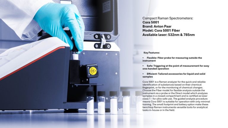
·         Measuring 3D, non-contact step heights from nanometers to millimetres

·         Capable of measuring film thickness of transparent film(s) using ZDot or ZFT measurement techniques.

·         Measures 3D texture, quantifying the sample’s roughness and waviness.

·         Measure the 2D and 3D shape or bow of a surface.

·         Measuring stress induced during the manufacture of devices with multiple layers, such as semiconductor or compound semiconductor devices.

·         Automated Optical Inspection (AOI) to rapidly inspect the sample, differentiate different defect types, and map defect density across the sample.

·         Defect review uses an inspection tool KLARF file to drive the stage to the defect locations

·         Supports metrology and inspection of patterned sapphire substrates

·         Supports Wafer-Level Chip Scale Packaging (WLCSP) and Fan-Out Wafer Level Packaging (FOWLP) metrology requirements

·         Measure topography changes induced by laser surface processing for semiconductors, LED, microfluidic devices, PCBs, and more.

·         Measure microfluidic devices fabricated in materials, such as silicon, glass, and polymers. The system quantifies the height, width, edge profile, and texture of channels, wells, and control structures


Operator

En. Amirul Iman Bin Zainudin
 (03-89217159/amiruliman@ukm.edu.my)

For further inquiries, please contact our officer at amiruliman@ukm.edu.my